Uncovering the Truth: Switch 2 Hardware Leak Revealed, Impacting Nintendo’s Gaming Future
The Anticipation for the Nintendo Switch 2 is Reaching Frenzy Levels
As the hype surrounding the Nintendo Switch 2 (or whatever it may end up being called) reaches a fever pitch, a major leak last week has given us our first hard evidence of what the machine might look like, and it’s painting a fascinating picture.
A Compelling Case for the Leak’s Accuracy
Thanks to the diligent efforts of members of the Famiboard forums, who have tracked down every leak and compiled a comprehensive specification, we can assume that the leak is genuine – at least as accurate as an old prototype from October 2023 can be. The evidence suggests that the Switch 2 will have a larger form factor, an 8-inch LCD, and new Joy-Cons connecting via magnetic rails.
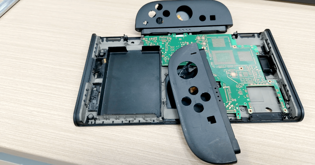
More Revelations from the Prototype Leak
The leak has also given us a glimpse into the internal workings of the Switch 2. We know that it’ll have twin USB-C ports, top and bottom, with the top one potentially reserved for peripherals, including an external camera. The console will also have a Micro-SD card slot, and we can hope that it supports the latest formats for bandwidth-heavy games. A 256GB UFS 3.1 storage module will come pre-installed, and cartridges are supported, along with strong hints that original Switch media will also be compatible.
The Mainboard Reveals Insights into the SoC and RAM
The mainboard provides a look at the architecture within. We see two pads for the 6GB LPDDRX 7500MT/s memory modules, giving us 12GB of RAM in total, with a 128-bit memory interface offering up a maximum of 102GB/s of bandwidth. The highly contentious SoC (System on Chip) is also visible, and we can try to glean clues about the technology used from its size.
Unraveling the Mystery of the T239 Processor
The T239 processor has been a subject of intrigue, with many speculating about its architecture and the process node used. A recent leak has revealed the existence of the T234 chip, created by Nvidia for its automotive endeavors and Jetson Orin NX kits. While the T234 chip is a whopping 455mm² in size, the T239 processor is much smaller and designed specifically for handheld use. Power efficiency is a major concern for the Switch 2, and if the T239 is built on an 8nm process, it could struggle to deliver optimal performance.
The Alternative: TSMC’s 5nm Process Node
An alternative theory is that the T239 is built on TSMC’s 5nm process node, used for Nvidia’s RTX 40-series graphics cards. This would be a significant development, delivering incredible efficiency, fast clocks, and tiny die area. However, it would also raise questions about the console’s design and battery life.
Nintendo’s Priorities: Price, Performance, and Power
Historically, Nintendo prioritizes price, performance, and power. Given the limitations of the T239 processor, it’s possible that the Switch 2 will use the 6nm process node used by the PS5, rather than the 4nm or 5nm process nodes. Heat dissipation and battery life may play a significant role in determining the final choice of process node.
The Art of Anticipation
In the end, we need to accept that Nintendo and Nvidia know what they’re doing. Despite the limitations of the Tegra X1 and a mostly awful showing on the Shield Android TV mini-console, the Switch went on to become a phenomenal success. Now, Nintendo faces the challenge of following that up, and we can only hope that they’ve learned from their past successes and challenges.