Samsung Foundry Unveils Ambitious Plan to Develop 2nm Chips in the US

TSMC’s 2nm Chip Production: A New Era for US Tech
In a significant development for the US tech industry, Taiwan Semiconductor Manufacturing Company (TSMC) plans to build 2nm chips at one of its US-based fabs in Arizona by 2028. This is excellent news for American tech companies like Apple, which will benefit from the cutting-edge technology. However, it’s worth noting that TSMC’s most advanced chips could be built in Taiwan using the 1.4nm node by then.
The Importance of Process Node Numbers
The process node used to build a chip is crucial because lower process node numbers typically result in smaller transistors packed inside a chip. This means that a chip’s transistor count can be higher, along with its transistor density, which is the number of transistors that fit into a given area of the component.
What Does This Mean for Chip Performance?
Typically, the more transistors shoehorned into a chip, the more powerful and energy-efficient that chip is. TSMC will start mass producing 2nm chipsets during the second half of this year. Apple is expected to be among the first to use a 2nm application processor to power a smartphone, with the iPhone 18 line featuring the A20 and A20 Pro application processors.
Samsung Foundry’s Plans
TSMC won’t be the only foundry in the US churning out 2nm SoCs. Samsung Foundry is planning to build an advanced chip production facility in Taylor, Texas. The company has invested billions in the fab and received $4.74 billion in incentives from the US government. Samsung Foundry hopes to start producing chips at the facility in 2026, with plans to manufacture 3nm and 2nm chips.
The Future of Chip Production in the US
As we’ve discussed before, TSMC is already building 4nm chipsets in Arizona, including the A16 Bionic for the iPhone 15 and iPhone 15 Plus. The company is also producing parts of Apple’s S9 system-in-package (SiP) processor for the Apple Watch Series 9. The difference between a SiP and a SoC is that the latter includes all of the components (CPU, GPU, memory, etc.) in a single die, while the SiP combines individual dies into a single package.
GAA Transistors: The Key to Improved Performance
Samsung Foundry employs Gate-All-Around (GAA) transistors for both 3nm and 2nm production. GAA uses horizontal nanosheets placed vertically as the gate, completely covering the channel on all four sides, reducing current leaks and improving the drive current. This results in greater performance and more energy efficiency for the chip. TSMC sticks with FinFET transistors for its 3nm chips and will use GAA at 2nm.
A New Era for US Chip Production
The US is finally getting its shot at becoming a major player in the production of advanced semiconductors. In ten years, many of the chips that Apple obtains for its devices might be built in fabs located in the United States. This is an exciting development for the tech industry, and we can expect to see significant advancements in chip production in the years to come.
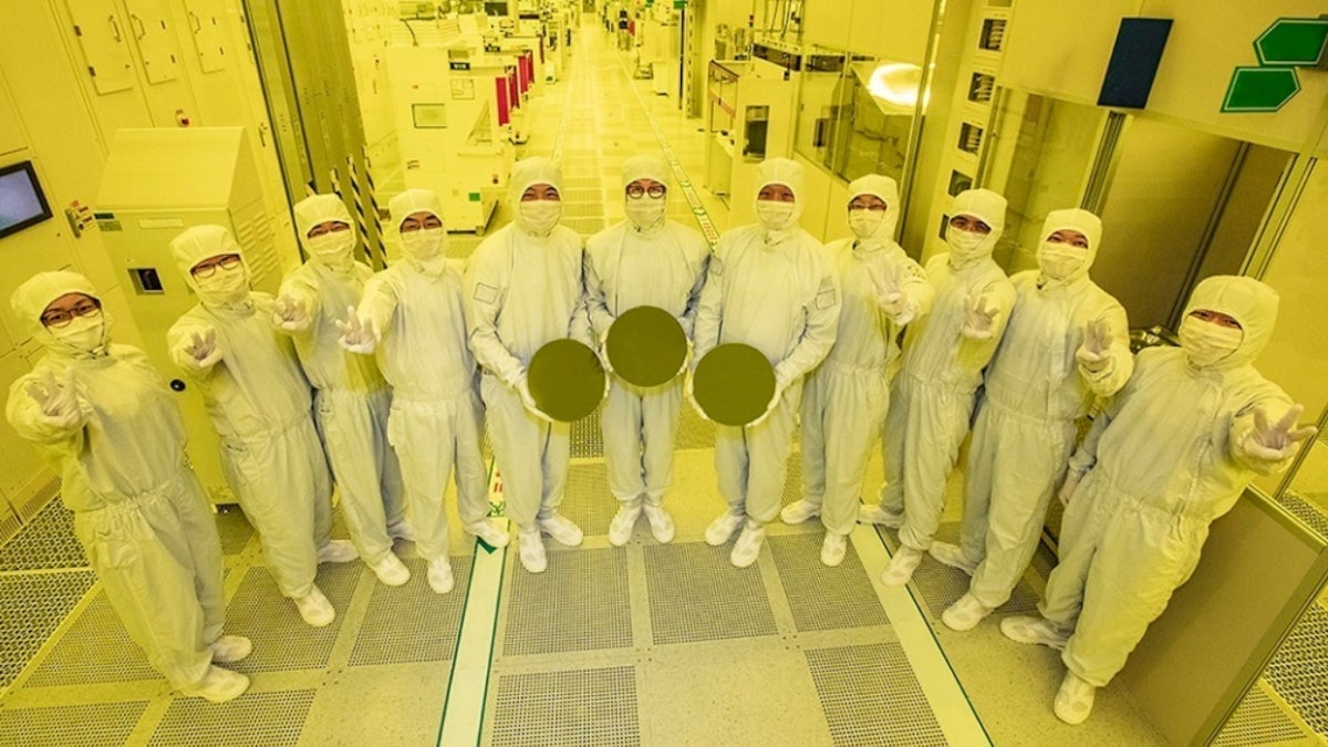
[Image: Samsung Foundry hopes to build 3nm and 2nm chips in Tyler, Texas. | Image credit-Samsung Foundry]


